Class D Amplifier with DSM Filter
This example shows how to model a class D amplifier and embed that amplifier in a delta-sigma modulator (DSM) filter using the Mixed-Signal Blockset. Many audio amplifiers use a class D amplifier as their output stage, and some of those audio amplifiers have very high fidelity requirements. One of the ways to increase the fidelity of a class D amplifier is to embed it in a DSM filter. This example offers you efficient methods for modeling such a circuit and optimizing its performance.
Class D Amplifier
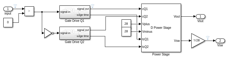
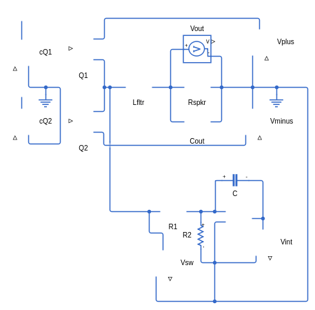
The class D amplifier circuit topology used in this example is the half bridge topology shown in the Simscape diagram below. The half bridge is created by transistors Q1 and Q2, the speaker load is represented by the resistor Rspkr, and the lowpass filtering is performed by Lfilter and Cout.
circuitmodel='HalfBridgeDAmp';
load_system(circuitmodel);
open_system(circuitmodel);
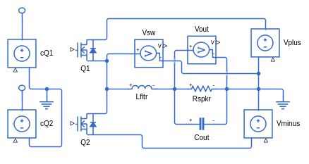
The power supplies are modeled by the voltage sources Vplus and Vminus. The voltage applied to the speaker is Vout and the output voltage of the half bridge is Vsw. In this model the transistors are modeled using the Ideal MOSFET model, which uses logical rather than electrical gate drive signals. The gate drive signals are brought into the model using the voltage sources cQ1 and cQ2, with the convention that the gate drive for a transistor is identified as a voltage source whose designator is the letter 'c' followed by the designator of the transistor being driven. cQ1 drives Q1 and cQ2 drives Q2.
The following Simulink model contains an MSB SwitchedCircuit block labeled "D Power Stage" that models the circuit in the Simscape diagram. The block contains closed form solutions to Kirchhoff's equations for the circuit for each possible combination of transistor states. The block also provides a circuit debug feature.
model='HalfBridgeDAmp_OL';
load_system(model);
open_system(model);
Model 'HalfBridgeDAmp_OL' was exported from R2026b to R2026a. To find blocks that were removed during the export operation, <a href="matlab:slexportprevious.utils.displayReplacedBlocks('HalfBridgeDAmp_OL')">click here</a>. Save the model to remove this notification.
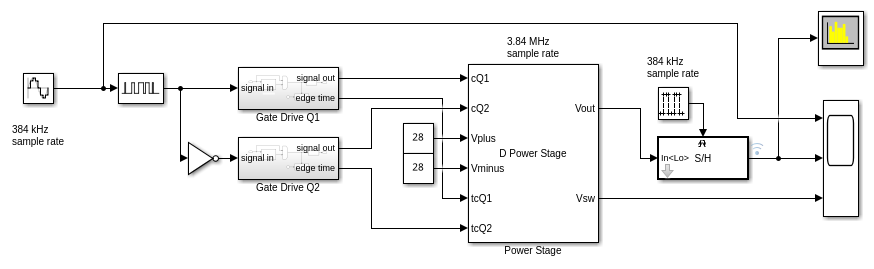
To build or rebuild the Power Stage block in this model, first create a CircuitConfiguration object (cktobj below) and then use that object to build the block in the model. Since this block defines the sample rate for the model, the InheritSampleRate and SampleRate parameters must be set.
cktobj = cktconfig(circuitmodel,...
    CircuitDesignName = "D Power Stage",...
    BlockName = "Power Stage",...
    Ports = {'cQ1','cQ2','Vplus','Vminus','Vout','Vsw'});
blockpath = cktblock(cktobj,model);
set_param(blockpath,'InheritSampleRate','off');
set_param(blockpath,'SampleRate','10*384e3');
Note that in this model the switching frequency of the amplifier is 384 kHz, and so the sample rate must be ten times that frequency to accommodate a duty cycle range between 0.1 and 0.9.
The model also contains a spectrum analyzer to offer more insight into the amplifier performance. For efficient execution when including the spectrum analyzer, the output of the amplifier is resampled at 384 kHz and the input sine wave is sampled at the same rate. This solution produces satisfactory results because the cutoff frequency of the amplifier's filter is 25 kHz.
The gate control signals for the circuit are generated by a pulse width modulator followed by gate drive subsystems that measure and output the precise transition times (tcQ1 and tcQ2) for the gate control signals along with the control signal value at each sample time. The Power Stage block uses the transition times to model the precise timing of the gate control signals.
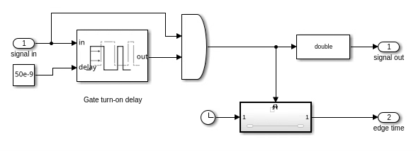
In a real circuit it is essential that the gate control "on" transitions are delayed with respect to the "off" transitions so that no two transistors are ever both conducting at the same time. As shown below, the gate drive subsystems include a model of the gate delay circuit that closely resembles one common circuit design. The gate delay is 50ns.
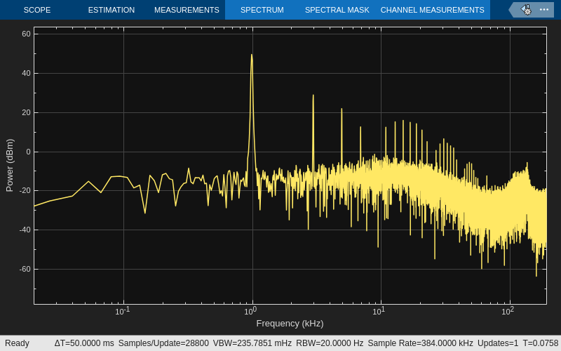
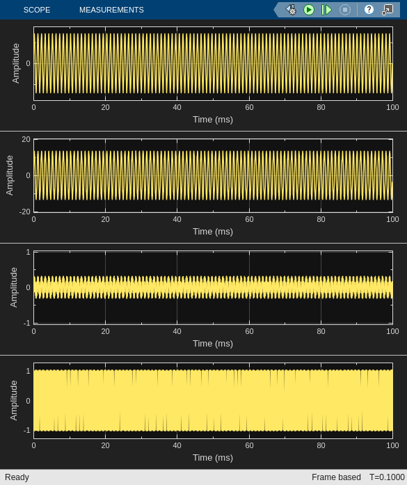
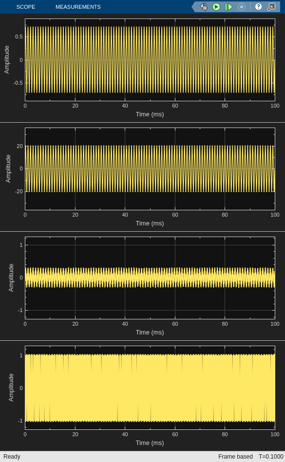
Running the model with a sine wave peak input amplitude of 0.35 produces the following voltage waveform and spectrum.
sim(model);
open_system([model,'/Time Scope']);
open_system([model,'/Spectrum Analyzer']);
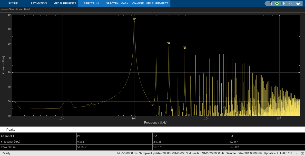
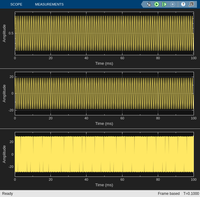
Note that the measured spectrum contains evidence of nonlinear distortion and possibly other forms of distortion as well. You can explore the nonlinear distortion by rerunning this model with amplitudes less than 0.35, including an amplitude of 0.
Transfer Function and Gain Distortion
It is well known that the gate delay in the class D amplifier gate drive causes nonlinear distortion in the output signal [1]. You can analyze this distortion by performing an operating point analysis. The operating point analysis also produces a small signal model that can be used to evaluate the transfer function of the circuit or model the circuit in a control system analysis. After having executed at least the first two sections of the script in the previous section, use the cktoperpoint function to perform the operating point analysis. The operating point analysis produces the following plot.
[dcresults,plotdata,waves,ssmodels,abcd] = cktoperpoint(cktobj, ...
    OutputPort = 'Vout',...
    ControlVariable = "Duty cycle", ...
    DutyCycle = [0.1 0.9], ...
    Frequency = 384e3, ...
    PhaseOffsets = '[0,d]', ...
    PulseDuration = '[d-50e-9*1e5,1-d-50e-9*1e5]', ...
    WaveSamples = 1024, ...
    OutputValues = 0, ...
    InputValues = {"Vplus",28;"Vminus",28});
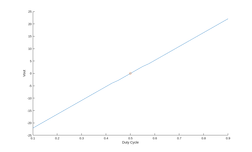
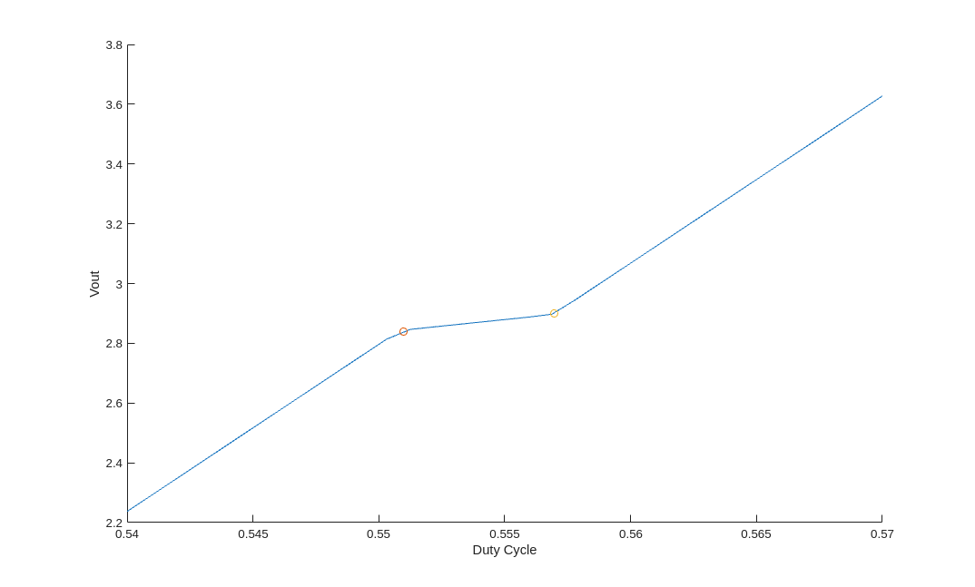
In this plot a small amount of nonlinear distortion is visible near a duty cycle of 0.45 and 0.55. You can get a more detailed view of the nonlinear distortion in that region by modifying the operating point analysis to concentrate on the region between 0.54 and 0.57.
[dcresults,plotdata,waves,ssmodels,abcd] = cktoperpoint(cktobj, ...
    OutputValues = [2.84,2.9], ...
    DutyCycle = [0.54 0.57]);
Close the current figure so that it does not get re-displayed later in this example.
close;
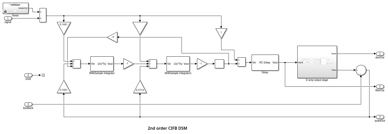
DSM Filter
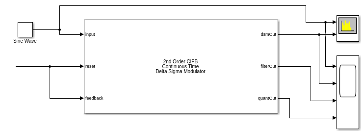
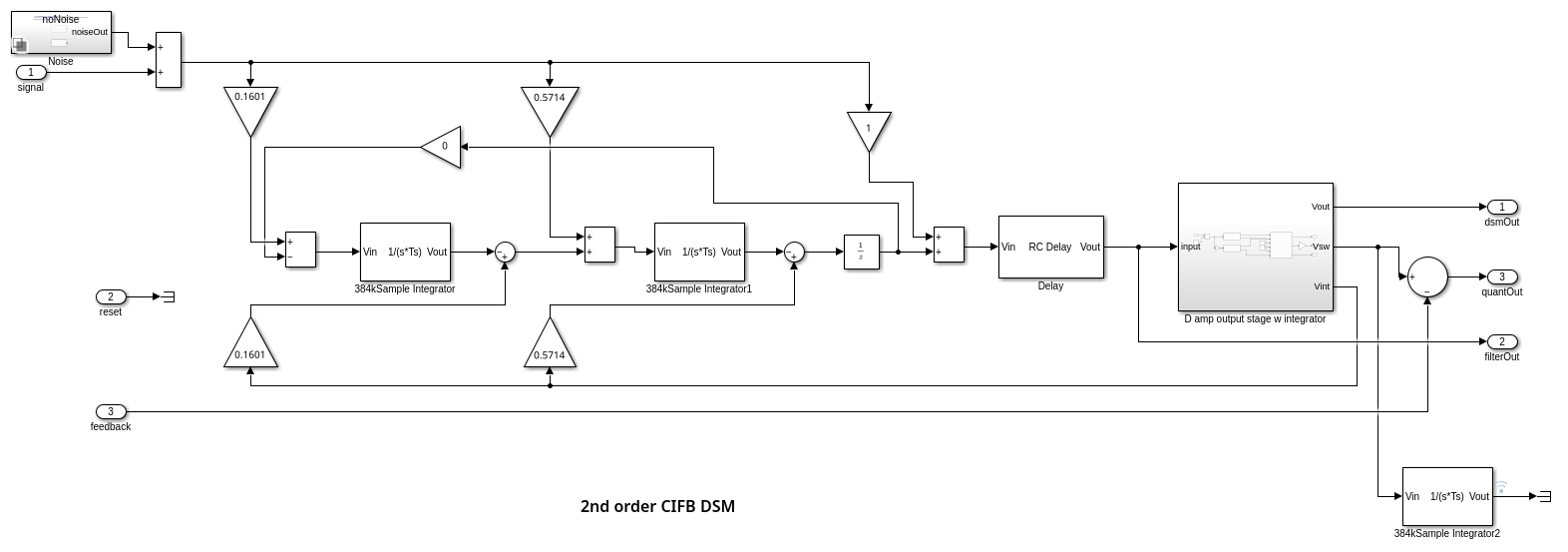
One of the ways to reduce the effect of gate delay nonlinearities and other impairments is to embed the class D amplifier inside a DSM filter. You can model this arrangement by using a Delta Sigma Modulator block from Mixed-Signal Blockset™ and then modify its structure by replacing the quantizer in that model with the class D amplifier.One common practice is to use the saturated waveform at the output of the amplifier's half bridge or full bridge as the feedback signal otherwise produced by the quantizer, scaling the amplitude of that signal down to a more typical quantizer output amplitude. However as will be demonstrated in this section, it is important to include detailed behaviors such as gate delays and body diode forward voltages in the feedback signal to obtain the maximum benefit from the DSM filtering. This requires continuous time rather than discrete time processing such as is implemented in the MSB Continuous Time Delta Sigma Modulator block. This section shows you how to transform a second order continuous time CIFB DSM modulator into a class D amp with DSM filtering.
dsmModel='CT_DSM_2ndOrder';
open_system(dsmModel);
Configure the Continuous Time Delta Sigma Modulator to an over-sampling ratio (OSR) of 9 and a system bandwidth of 384e3/18, which is slightly greater than the desired audio system bandwidth of 20kHz. This combination sets the sample rate to the desired 384kHz amplifier switching frequency and sets the filter coefficients to the appropriate values.
Click the "Edit system" option at the top of the block mask and accept the warning associated with this action. Descend through two layers of the subsystem to get to the implementation of the DSM filter. Copy the contents of this view into a new subsystem that will be the starting point for your DSM class D amplifier.
editModel = 'CT_DSM_2ndOrder_for_edit';
load_system(editModel);
open_system([editModel,'/CT 2nd order DSM'],'force','tab');
Model 'CT_DSM_2ndOrder_for_edit' was exported from R2026b to R2026a. To find blocks that were removed during the export operation, <a href="matlab:slexportprevious.utils.displayReplacedBlocks('CT_DSM_2ndOrder_for_edit')">click here</a>. Save the model to remove this notification.
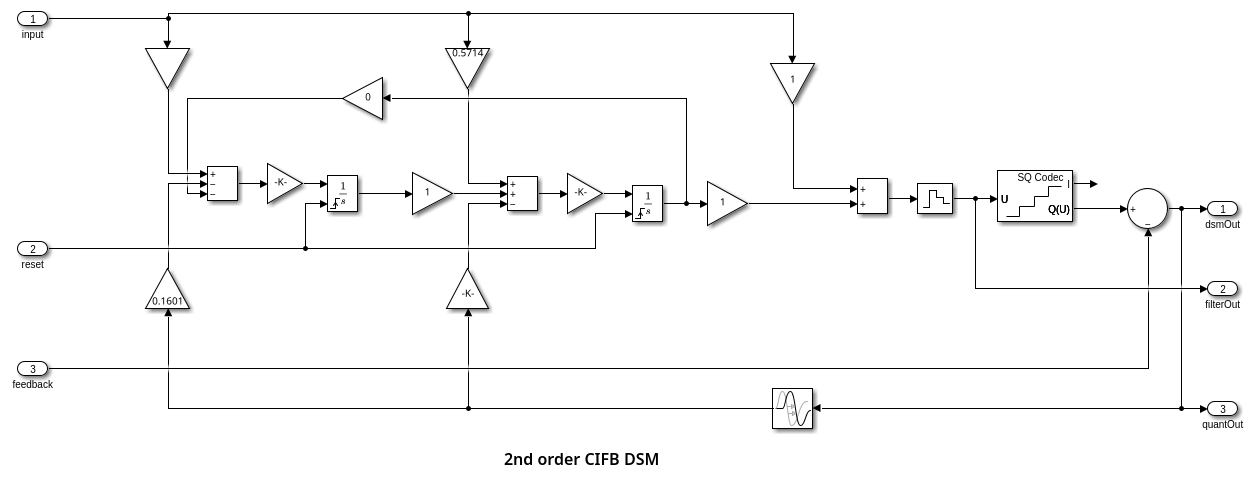
This view contains the basic filter structure and the filter coefficients needed in your model. However there are several changes that are either essential or will significantly improve the clarity of your model.
Replace the quantizer with a class D amplifier.
While class D amplifier resembles a quantizer in the sense that its half bridge output Vsw is a saturated waveform like that of a quantizer, the quantizer is a clocked circuit whereas in its unfiltered form the class D amplifier depends on the PWM driving the gate drivers for this function. While there are design options for supplying a synchronous substitute for the PWM in the DSM application, there is a simpler option that produces an asynchronous DSM. The class D amplifier becomes the gain stage for a ring oscillator and, with some additional delay, the DSM feedback network provides the delay that determines the ring oscillator's frequency of oscillation.
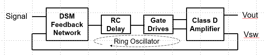
In this design the class D amplifier itself and the gate drives have been copied from the unfiltered class D amplifier earlier in this example.
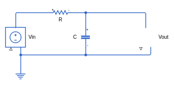
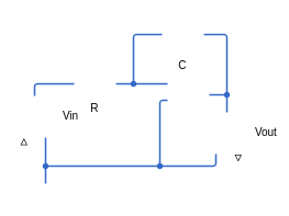
The RC delay circuit is a single stage network with a time constant of 1.5e-7, which is only a small fraction of the 2.6e-6 period of the desired oscillation rate.
rcModel='RCdelay';
load_system(rcModel);
open_system(rcModel);
Model 'RCdelay' was exported from R2026b to R2026a. To find blocks that were removed during the export operation, <a href="matlab:slexportprevious.utils.displayReplacedBlocks('RCdelay')">click here</a>. Save the model to remove this notification.
The DSM model is also improved by replacing the "continuous time" integrators and their input gain blocks (whose gains are equal to the DSM sample rate) with MSB LinearCircuit discrete time models of the actual integrator circuit.
The required frequency response is 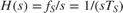 . The frequency response of the op-amp integrator is approximately
  . The design equation is
  .
.
Like the Class D Amplifier model, the IntegratorCircuit model adjusts its coefficients at run time based on the discrete sample time, to produce time domain results that are as accurate as possible given the sample time.
integratorModel='IntegratorCircuit';
load_system(integratorModel);
open_system(integratorModel);
The resulting asynchronous DSM with class D amplifier is shown below.
classDModel='Async_DSM_2ndOrder_plus_DAmp';
load_system(classDModel);
open_system([classDModel,'/Continuous Time Delta Sigma Modulator'],'force','tab');
Model 'Async_DSM_2ndOrder_plus_DAmp' was exported from R2026b to R2026a. To find blocks that were removed during the export operation, <a href="matlab:slexportprevious.utils.displayReplacedBlocks('Async_DSM_2ndOrder_plus_DAmp')">click here</a>. Save the model to remove this notification.
Within the class D amplifier subsystem a gain of 1/128 has been inserted in the Vsw path to make its output amplitude comparable to that of the quantizer it is replacing.
open_system([classDModel,'/Continuous Time Delta Sigma Modulator/D amp output stage'],'force','tab');
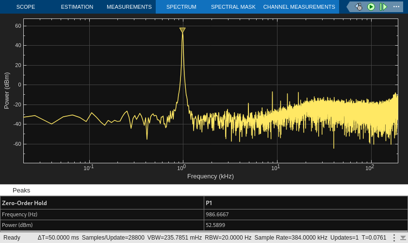
The resulting output spectrum is
sim(classDModel);
open_system([classDModel,'/Spectrum Analyzer'],'force','tab');
While there is evidence of significant filtering, the result isn't as good as might be desired. The nonlinear distortion, especially for the third harmonic, is significant and the noise floor is not as low as desired. One of the limitations of this model is that the input to the integrators is sampled at only ten times the switching frequency of the amplifier. This sample rate could be increased, but simulation execution time would increase to an impractical level. Another approach to this problem is to place the integrator of the amplifier output inside the SwitchedCircuit object for the output stage. The SwitchedCircuit object class is designed to evaluate the effect of multiple switch state transitions within a single sample interval. If the integrator for the half bridge output is inside the SwitchedCircuit object, then its input and output will be updated whenever there is a gate delay or a body diode transition. The effect may be small, but it could be significant. The diagram for a class D amplifier output stage with feedback integrator is shown below. The integrator circuit is the same as that used already in the DSM filter, except that it has a Resistive divider at its input to reduce the effective input amplitude to one volt.
open_system('HalfBridgeDAmp_plus_Integrator');
%
The continuous time DSM with D amp output was modified to split each integrator into a pair of integrators, as described in [2]. One integrator in an integrator pair has the filter signals as its inputs while the other integrator has the D amp output as its input. The integral of the D amp output is the same for both integrators in the filter, and so the one D amp integrator is shared between the integrator pairs for both filter stages.
classDintModel='Async_DSM_2ndOrder_DAmp_Integrator';
load_system(classDintModel);
open_system([classDintModel,'/Continuous Time Delta Sigma Modulator'],'force','tab');
Model 'Async_DSM_2ndOrder_DAmp_Integrator' was exported from R2026b to R2026a. To find blocks that were removed during the export operation, <a href="matlab:slexportprevious.utils.displayReplacedBlocks('Async_DSM_2ndOrder_DAmp_Integrator')">click here</a>. Save the model to remove this notification.
In this model the integrator outputs are logged at multiple points in the filter to monitor integrator output amplitudes. An integrator has also been added to integrate the half bridge switching waveform externally, as in the previous model. You can view these logged signals in the Simulink Data Inspector.The resulting spectrum is shown below.
sim(classDintModel);
open_system([classDintModel,'/Spectrum Analyzer'],'force','tab');
While there is still a little bit of third order nonlinear distortion evident, If you examine the logged signals in the Simulink Data Inspector you will note that the output amplitude of each half of an integrator pair gets as high as +-40V. However in the real circuit the amplitude at the output of each integrator in the filter is the summing junction output for the corresponding integrator pair in the model. That summing junction output stays within +-1V. These results suggest that in the DSM filter for a class D amplifier it is critical to make the inputs to the filter's integrators reflect even second order impairments in the amplifier's switching bridge.
References
1. Jun Honda and Jonathan Adams, "Class D Audio Amplifier Basics", Application Note AN-1071, International Rectifier, Infineon.com.
2. Pavan, Schreier and Temes, Understanding Delta-Sigma Data Converters, Second Edition, section 8.1, IEEE, copyright 2017.