Digital Timing Using Fixed Step Sampling
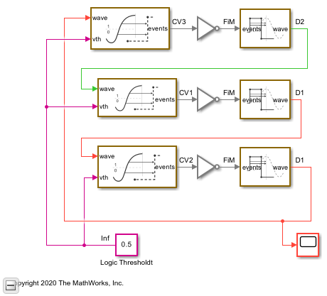
This example shows how to model a three-stage ring oscillator using a combination of fixed-step and variable-step discrete sample times.
For each stage of the ring oscillator, the Logic Decision block converts the input into a saturated variable step discrete signal and the Slew Rate block converts the output to an analog fixed step discrete signal. Some delay in the Logic Decision block is unavoidable; however most of the delay is introduced by the Slew Rate block.
The Logic Decision block generates a variable step discrete sample at its output in response to any threshold crossing it detects at its input.
For a fixed step discrete input sample time, the threshold crossing time is determined by linear interpolation between the two most recent samples. The output sample is delayed by one sample because the block does not have access to the fixed in minor step services of an ODE solver. In the modeling of a circuit, this delay must represent either the delay of input stages in a multi-stage transistor circuit or RC transmission line routing delay.
For a fixed step input, the precision of the threshold crossing time reported by the Logic Decision block depends on the ratio of the spectral content of the signal to the Nyquist frequency defined by sample rate. For a sine wave at 0.25 times the Nyquist frequency (8x oversampling), the maximum error in the reported threshold crossing time is 1% of a sample interval. For 0.1 times the Nyquist frequency, the maximum error is 0.15% of a sample interval. For applications requiring greater precision, such as evaluating low level phase noise at the output of a PLL, an approach that depends only on variable step sampling may produce more precise results.
For a variable step input, the output of the Logic Decision block is delayed by the minimum delay parameter for the block.
The Slew Rate block implements a linear time invariant transfer function that can be applied to either a variable step or fixed step input signal, producing a fixed step discrete output signal with a sample time that was set by the Slew Rate block. The delay of the Slew Rate block is a mixture of:
Constant delay such as might occur in a multi-stage transistor circuit or RC routing delay
Nearly constant slew rate such as would be typical of a saturated transistor driving a capacitive load
Exponential decay such as would be typical of an RC circuit
Load the mixed analog/digital model and update the model to display sample times.
open_system('AnalogWaveform');
set_param(gcs,'SimulationCommand','update');
Slew Rate Block in Default Sampling Mode
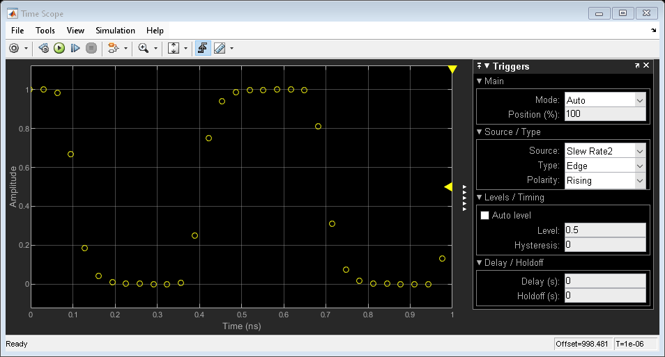
In this section, use the Default sampling mode of the Slew Rate block to model the response of a circuit whose slew rate is nearly constant, such a saturated transistor driving a capacitive load.
For this section, the Slew Rate blocks are configured to their Default sampling mode, which maximizes the portion of the delay due to nearly constant slew rate (saturated transistor) and minimizes the delay due to constant delay or exponential decay.
The delay for one logic stage is set to a slightly different value than for the other stages so that the model enters the correct mode of oscillation.
Since the model contains no differential equations, the solver is Variable Step Discrete.
Note in the response that the onset of the switching edges is slightly rounded. In a real circuit, this would typically be due to the RC response of the routing.
Run the mixed analog/digital model with default sample times.
sim('AnalogWaveform');
Slew Rate Block in Advanced Sampling Mode
In this section, use the Advanced sampling mode of the Slew Rate block to model circuits whose response is primarily a decaying exponential.
Choose the Advanced mode for the Slew Rate block sampling and set the Maximum frequency of interest to a value that is high enough to make the delay of the Slew Rate block due primarily to exponential decay. This choice also minimizes the delay of the Logic Decision block.
Note in the response that the onset of the switching edges is relatively sharp.
Configure the mixed analog/digital model to approximate single pole response.
% Slew Rate1
set_param('AnalogWaveform/Slew Rate1','DefaultOrAdvanced','Advanced');
set_param('AnalogWaveform/Slew Rate1','MaxFreqInterest','20e9');
set_param('AnalogWaveform/Slew Rate1','RisePropDelay','92e-12');
set_param('AnalogWaveform/Slew Rate1','RiseTime','15.5e-11');
% Slew Rate2
set_param('AnalogWaveform/Slew Rate2','DefaultOrAdvanced','Advanced');
set_param('AnalogWaveform/Slew Rate2','MaxFreqInterest','20e9');
set_param('AnalogWaveform/Slew Rate2','RisePropDelay','92e-12');
set_param('AnalogWaveform/Slew Rate2','RiseTime','15.5e-11');
% Slew Rate3
set_param('AnalogWaveform/Slew Rate3','DefaultOrAdvanced','Advanced');
set_param('AnalogWaveform/Slew Rate3','MaxFreqInterest','20e9');
set_param('AnalogWaveform/Slew Rate3','RisePropDelay','95e-12');
set_param('AnalogWaveform/Slew Rate3','RiseTime','16e-11');
Update the diagram to show the revised sample times in the sample time legend.
set_param(gcs,'SimulationCommand','update');
Run he mixed analog/digital model with emphasized one pole response.
sim('AnalogWaveform');