RF Wideband Bandpass Tunable Filter with Re-configurable In-Band Characteristics
Tunable RF and Microwave Filters are pivotal components in modern communication and radar systems, offering the unique ability to dynamically adjust their frequency response to meet varying operational demands. These filters enable the selective passage of signals within a certain frequency range while blocking others, a crucial function for optimizing system performance in real-time.
In this MATLAB example, we explore the capabilities of the RF PCB Toolbox to model and simulate tunable RF filters, focusing on the impact of varying capacitance values on the filter's frequency response. By adjusting the capacitance of the capacitors integrated into the filter design, we can dynamically tune the filter's operating frequency, showcasing a practical application of tunable RF filters in real-world scenarios.
Define the Variables
Define the variables to create the top metal layer for the filter. This top layer will be designed using the shape catalog in the RF PCB Toolbox, with dimensions maintained according to the reference paper.
%Za dimensions
Za_Length=45.25e-3;
Za_Width=1.8e-3;
%Z1 dimensions
Z1_Space=22e-3;
Z1_Width=32.9e-3;
Z1_Length=6.2e-3;
%Z2 dimensions
Z2_Width=29.3e-3;
Z2_Length=4.96e-3;
Z2_Edge=Z1_Width+Za_Width+Z2_Width;
%gnd dimensions
gndL=90.5e-3;
gndW=0.1;
%U1 ubend dimensions
U1_Length=[25.1e-3 8e-3 25.1e-3];
U1_Width=4.5e-3;
U1_Diag=4.5e-3*sqrt(2);
U1_Space=2.75e-3;
%L1 bend dimensions
L1_Length=[10.25e-3 46.45e-3];
L1_Width=4.5e-3;
L1_Diag=4.5e-3*sqrt(2);
L1_Space=2.75e-3;

Za=traceRectangular(Length=Za_Length,Width=Za_Width,...
    Center=[-gndL/2+Za_Length/2 Za_Width/2]);
%z1
Z1=traceRectangular(Length=Z1_Length,Width=Z1_Width+Za_Width,...
    Center=[-gndL/2+Z1_Space+Z1_Length/2 (Z1_Width/2+Za_Width/2)]);
%Z2
Z2=traceRectangular(Length=Z2_Length,Width=Z1_Width+Za_Width+Z2_Width,...
    Center=[-gndL/2+Z1_Space+Z1_Length/2 (Z1_Width/2+Za_Width/2+Z2_Width/2)]);
Create the Filter geometry
Use the shape catalog in RF PCB Toolbox to create the top layer of the filter. As the filter structure has U bends and rectangles, ubendMitered shape and traceRectangular can be used to create the metal layer. Add the shapes using the boolean add to create the left section of the filter.
U1=ubendMitered;
U1.Length=U1_Length;
U1.Width=[U1_Width U1_Width U1_Width];
U1.MiterDiagonal=U1_Diag;
U1_Xcord=-gndL/2+Z1_Space+Z1_Length/2+U1_Width/2+U1_Length(2)/2;
U1_Ycord=Z2_Edge+U1_Space+U1_Length(1);
U1.ReferencePoint=[U1_Xcord U1_Ycord];
U1 = rotateX(U1,180);
L1=bendMitered;
L1.Length=L1_Length;
L1.Width=[L1_Width L1_Width];
L1.MiterDiagonal=L1_Diag;
L1_Xcord=-gndL/2+Z1_Space+Z1_Length/2-Z2_Length/2-L1_Space-L1_Length(1);
L1_Ycord=Z2_Edge;
L1.ReferencePoint=[L1_Xcord L1_Ycord];
L1 = rotateY(L1,180);
%b1 dimensions
b1_Width=4.5e-3;
b1_Length=4.5e-3;
b1_Space=2.75e-3;
b1_Xcord=-gndL/2+Z1_Space+Z1_Length/2+U1_Width+U1_Length(2);
b1_Ycord=Z2_Edge-b1_Width/2;
b1=traceRectangular(length=b1_Length,Width=b1_Width,Center=[b1_Xcord b1_Ycord]);
%b2 dimensions
b2_Width=4.5e-3;
b2_Length=4.5e-3;
b2_Xcord=L1_Xcord;
b2_Space=2.75e-3;
b2_Ycord=L1_Ycord-L1_Length(2)-b2_Space-b2_Width/2;
b2=traceRectangular(length=b2_Length,Width=b2_Width,Center=[b2_Xcord b2_Ycord]);
LeftSection=Za+Z1+Z2+U1+L1+b1+b2;
Visualize the left section using the show method and mirror this section to create the Right section and visualize it. Use the boolean add to add the two sections to create the complete filter geometry.
figure;
show(LeftSection);
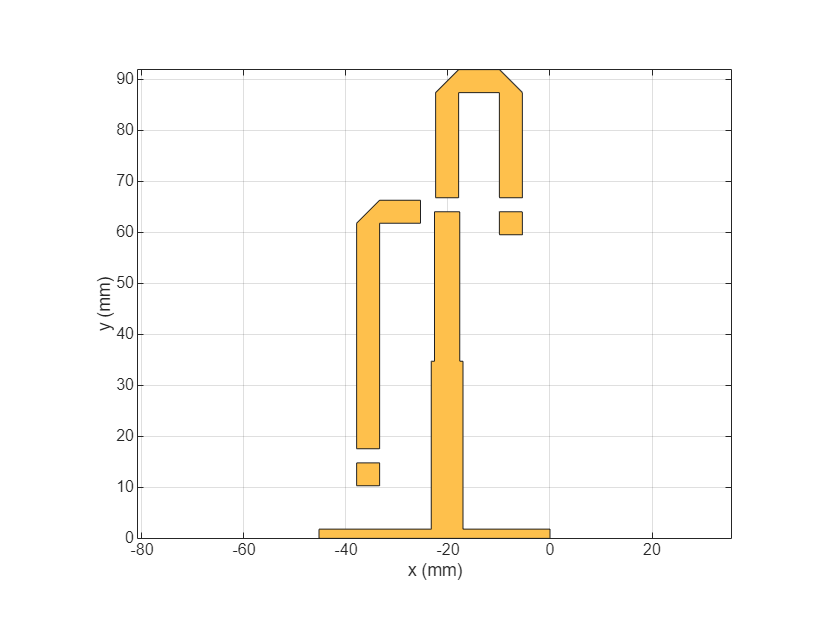
Use the mirrorY function to mirror the left section along the Y axis and visualize the right section.
RightSection = copy(LeftSection);
RightSection = mirrorY(RightSection);
figure;
show(RightSection)
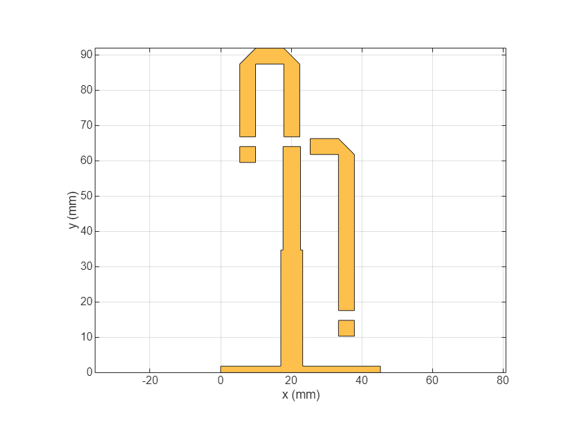
Combine the Left and Right Sections using boolean add and visualise the top layer of the filter.
combineSection = LeftSection + RightSection;
figure;
show(combineSection);

Create the pcbComponent
Use the pcbComponent to place the created top layer on the substrate and assign the ground plane. Assign the properties of the pcbComponent such as Layers, BoardShape, FeedLocations, FeedDiameter, ViaDiameter, ViaLocations and visualize the filter using show method.
S_Thick=1.27e-3;
substrate = dielectric(EpsilonR = 6.45,LossTangent = 0.0027,...
    Name = "custom",Thickness = 1.27e-3);

ground = traceRectangular(Length = gndL+2e-3,Width = gndW,...
    Center=[0,0.045]);
pcb = pcbComponent;
pcb.BoardShape = ground;
pcb.BoardThickness = 1.27e-3;
pcb.Layers ={combineSection,substrate,ground};
pcb.FeedDiameter = Za_Width;
%Feedlocations
delta = 0;
pcb.FeedLocations = [-gndL/2 0.9e-3 1 3;gndL/2 0.9e-3 1 3;Z1.Center(1) Z2_Edge-delta 1 3;Z1.Center(1) Z2_Edge+U1_Space+delta 1 3;...
   L1_Xcord+L1_Length(1)-delta Z2_Edge 1 3;L1_Xcord L1_Ycord-L1_Length(2)+delta 1 3;L1_Xcord L1_Ycord-L1_Length(2)-b2_Space-delta 1 3;...
   b1_Xcord b1_Ycord+b1_Width/2+b1_Space+delta 1 3;b1_Xcord b1_Ycord+b1_Width/2-delta 1 3;-Z1.Center(1) Z2_Edge-delta 1 3;-Z1.Center(1) Z2_Edge+U1_Space+delta 1 3;...
   -(L1_Xcord+L1_Length(1))+delta Z2_Edge 1 3;-L1_Xcord L1_Ycord-L1_Length(2)+delta 1 3;-L1_Xcord L1_Ycord-L1_Length(2)-b2_Space-delta 1 3;...
   -b1_Xcord b1_Ycord+b1_Width/2+b1_Space+delta 1 3;-b1_Xcord b1_Ycord+b1_Width/2-delta 1 3];
% Vias in pcb
ViaD=[];
ViaLocat=[];
startx=[b1_Xcord b2_Xcord -b1_Xcord -b2_Xcord];
starty=[b1_Ycord b2_Ycord b1_Ycord  b2_Ycord];
dist1=b2_Length/3;
d1=1e-3;
delx=[-1e-3  1e-3];
dely=[-1e-3 -1e-3 -1e-3 -1e-3 -1e-3 -1e-3];
for i=1:4
    p1=startx(i);
    p2=starty(i);
    for j=1:2
      ViaLocat=[ViaLocat;p1+delx(j) p2+dely(j)-delta+0.3e-3 1 3];
      ViaD=[ViaD d1];
    end
end
pcb.ViaLocations=ViaLocat;
pcb.ViaDiameter=ViaD;
figure;
show(pcb);
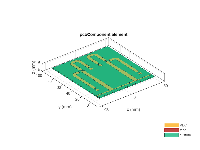
Use the mesh command to mesh the structure and give the MaxEdgeLength as 5 mm to create a dense mesh so that the finer gaps between the stubs can be meshed properly.
% load('pcb.mat')
figure,mesh(pcb,'MaxEdgeLength',8e-3);
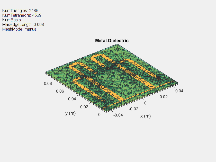
% figure,mesh(pcb);Use the Layout function to see the layout of the filter with the Vias and the Feed Locations. The feed locations other than the input and output will be connected to capacitors
figure;
layout(pcb);
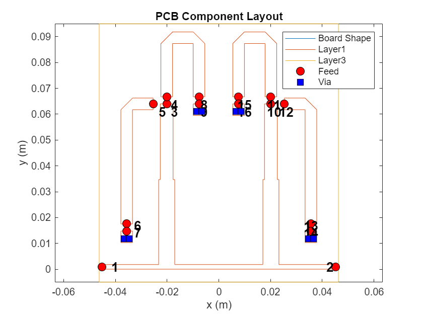
Use the sparameters function to calculate the S-Parameters of the pcbComponent with all the Feed Locations.
s=sparameters(pcb,linspace(0.4e9,1.4e9,101),50);
Create a pcbElement and convert to Circuit
Use the pcbElement to create a circuit with the S-Parameters and the Capacitors. Assign the Capacitor values to the PortValue property on the pcbElement.
C1 = capacitor(2.2e-12);
C2 = capacitor(2.2e-12);
Cr1 = capacitor(5.1e-12);
Cr2 = capacitor(1.6e-12);
C_1 = capacitor(2e-12);
C_2 = capacitor(2.2e-12);
C_r1= capacitor(5.1e-12);
C_r2= capacitor(1.6e-12);
pcbckt = pcbElement(pcb);
Warning: antenna.Polygon not supported for behavioral S-parameters.
pcbckt.AnalysisPorts = {1,2};
pcbckt.PortNumber = {{3,4},{3,5},{6,7},{8,9},{10,11},{10,12},{13,14},{15,16}};
pcbckt.PortValue = {C1,C2,Cr1,Cr2,C_1,C_2,C_r1,C_r2};
Sboard = sparameters(pcbckt,linspace(0.4e9,1.4e9,101),50);
figure;
rfplot(Sboard);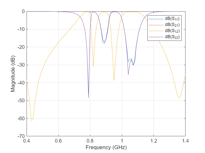
Results variation with different Capacitor values
Capacitance value is changed from the original value and the loop is run to multiply these capacitances from 1 to 10 times and the result is observed.
figure;
iterations = {'CapacitorValue','CapacitorValue*3','CapacitorValue*5','CapacitorValue*7'};
for i = 1:2:8
    C1 = capacitor(i*2.2e-12);
    C2 = capacitor(i*2.2e-12);
    Cr1 = capacitor(i*5.1e-12);
    Cr2 = capacitor(i*1.6e-12);
    C_1 = capacitor(i*2e-12);
    C_2 = capacitor(i*2.2e-12);
    C_r1= capacitor(i*5.1e-12);
    C_r2= capacitor(i*1.6e-12);
    pcbckt.AnalysisPorts = {1,2};
    pcbckt.PortNumber = {{3,4},{3,5},{6,7},{8,9},{10,11},{10,12},{13,14},{15,16}};
    pcbckt.PortValue = {C1,C2,Cr1,Cr2,C_1,C_2,C_r1,C_r2};
    Sboard = sparameters(pcbckt,linspace(0.4e9,1.4e9,101),50);
    S21 = rfparam(Sboard,2,1);
    plot(Sboard.Frequencies,10*log10(abs(S21)),"LineWidth",2);
    hold on
end
legend(iterations)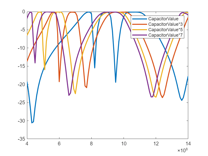
Use the Modelethics SELECT+ Library and use the capacitors from that database in the simulation.
mdlxSetup('C:\Modelithics\MATLAB')
mdlx = mdlxLibrary;
pobj2_0 = mdlxPart(mdlx,'600S','Capacitors','ATC','Rogers4350B4mil',Value=2e-12);
pobj2_2 = mdlxPart(mdlx,'600S','Capacitors','ATC','Rogers4350B4mil',Value=2.2e-12);
pobj5_1 = mdlxPart(mdlx,'600S','Capacitors','ATC','Rogers4350B4mil',Value=5.1e-12);
pobj1_6 = mdlxPart(mdlx,'600S','Capacitors','ATC','Rogers4350B4mil',Value=1.6e-12);
pcbckt.AnalysisPorts = {1,2};
pcbckt.PortNumber = {{3,4},{3,5},{6,7},{8,9},{10,11},{10,12},{13,14},{15,16}};
pcbckt.PortValue = {pobj2_2,pobj2_2,pobj5_1,pobj1_6,pobj2_0,pobj2_2,pobj5_1,pobj1_6};
Sboard = sparameters(pcbckt,linspace(0.4e9,1.4e9,91),50);
figure,rfplot(Sboard);
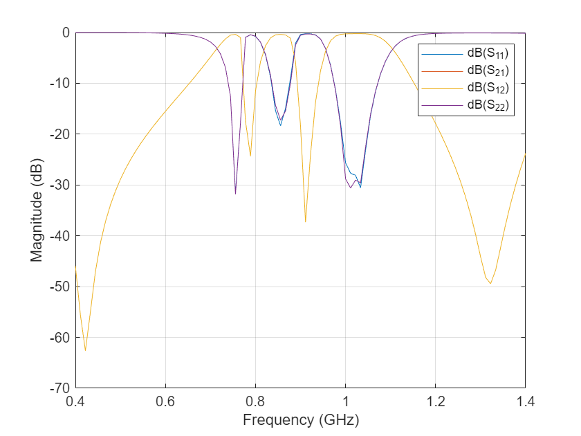
This workflow can be applied to connect passive and active component and simulate them with an RF PCB Layout and overall s-parameters can be computed.
References
[1] D. Psychogiou, R. Gómez-García and D. Peroulis, "RF Wide-Band Bandpass Filter With Dynamic In-Band Multi-Interference Suppression Capability," in IEEE Transactions on Circuits and Systems II: Express Briefs, vol. 65, no. 7, pp. 898-902, July 2018, doi: 10.1109/TCSII.2017.2726145
