P-Channel MOSFET
P-Channel metal-oxide-semiconductor field-effect transistor using either Shichman-Hodges equation or surface-potential-based model
Libraries:
Simscape /
Electrical /
Semiconductors & Converters
Description
The P-Channel MOSFET block provides two main modeling options:
Based on threshold voltage — Uses the Shichman-Hodges equation to represent the device. This modeling approach, based on threshold voltage, has the benefits of simple parameterization and simple current-voltage expressions. However, these models have difficulty in accurately capturing transitions across the threshold voltage and lack some important effects, such as velocity saturation. For details, see Threshold-Based Model.
This modeling option provides four ways of parameterizing an P-Channel MOSFET:
By specifying parameters from a datasheet.
By specifying equation parameters directly.
By a 2-D lookup table approximation to the I-V (current-voltage) curve. For details, see Representation by 2-D Lookup Table.
By a 3-D lookup table approximation to the I-V (current-voltage) curve that includes temperature data. For details, see Representation by 3-D Lookup Table.
Based on surface potential — Uses the surface-potential equation to represent the device. This modeling approach provides a greater level of model fidelity than the simple square-law (threshold-voltage-based) models can provide. The tradeoff is that there are more parameters that require extraction. For details, see Surface-Potential-Based Model.
Together with the thermal port variants (see Thermal Port), the block therefore provides you with four choices. To select the desired modeling option, set the Modeling option parameter to either:
Threshold-based — Basic model, which represents the device using the Shichman-Hodges equation (based on threshold voltage) and does not simulate thermal effects. This is the default.
Threshold-based with thermal — Model based on threshold voltage and with exposed thermal port.
Surface-potential-based — Model based on surface potential. This model does not simulate thermal effects.
Surface-potential-based with thermal — Thermal modeling option of the model based on surface potential.
Threshold-Based Model
The threshold-based modeling option of the block uses the Shichman and Hodges equations [1] for an insulated-gate field-effect transistor to represent a P-Channel MOSFET.
The drain-source current, IDS, depends on the region of operation:
In the off region (–VGS < –Vth) the drain-source current is:
In the linear region (0 < –VDS < –VGS +Vth) the drain-source current is:
In the saturated region (0 < –VGS +Vth < –VDS) the drain-source current is:
In the preceding equations:
K is the transistor gain.
VDS is the negative drain-source voltage.
VGS is the gate-source voltage.
Vth is the threshold voltage. For the four terminal parameterization, Vth is obtained using these equations:
VBS Range Vth Equation λ is the channel modulation.
To specify the parallel conductance of the channel, connect an Environment Parameters block to the electrical network. Then, set the minimum conductance of the P-Channel MOSFET block and other SPICE-compatible blocks by setting the GMIN parameter of the Environment Parameters block.
Charge Model for Threshold-Based Modeling Option
The block models capacitances either by fixed capacitance values, or by tabulated values as a function of the drain-source voltage. In either case, you can either directly specify the gate-source and gate-drain capacitance values, or let the block derive them from the input and reverse transfer capacitance values. Therefore, the Parameterization options for charge model on the Capacitance setting are:
Specify fixed input, reverse transfer and output
              capacitance
— Provide fixed parameter values from datasheet and let the block convert the input and reverse transfer capacitance values to capacitance values, as described below. This is the default method.Specify fixed gate-source, gate-drain and drain-source capacitance— Provide fixed values for capacitance parameters directly.Specify tabulated input, reverse transfer and output capacitance— Provide tabulated capacitance and drain-source voltage values based on datasheet plots. The block converts the input and reverse transfer capacitance values to capacitance values, as described below.Specify tabulated gate-source, gate-drain and drain-source capacitance— Provide tabulated values for capacitances and drain-source voltage.
Use one of the tabulated capacitance options (Specify tabulated input, reverse
transfer and output capacitance or Specify tabulated
gate-source, gate-drain and drain-source capacitance) when the datasheet
provides a plot of capacitances as a function of drain-source voltage. Using tabulated
capacitance values gives more accurate dynamic characteristics and avoids the need for
iterative tuning of parameters to fit the dynamics.
If you use the Specify fixed gate-source, gate-drain and drain-source
capacitance or Specify tabulated gate-source, gate-drain and
drain-source capacitance option, the Capacitance
setting lets you specify the Gate-drain capacitance, Cgd,
Gate-source capacitance, Cgs, and Drain-source capacitance,
Cds parameter values (fixed or tabulated) directly. Otherwise, the block
derives them from the Input capacitance, Ciss, Reverse
transfer capacitance, Crss, and Output capacitance, Coss
parameter values. These two parameterization methods are related as follows:
CGD = Crss
CGS = Ciss – Crss
CDS = Coss – Crss
For the four terminals parameterization, the Input capacitance, Ciss, Reverse transfer capacitance, Crss, and Output capacitance, Coss are obtained using these equations:
CGD = Crss
CGS + CGB = Ciss – Crss
CDB = Coss – Crss
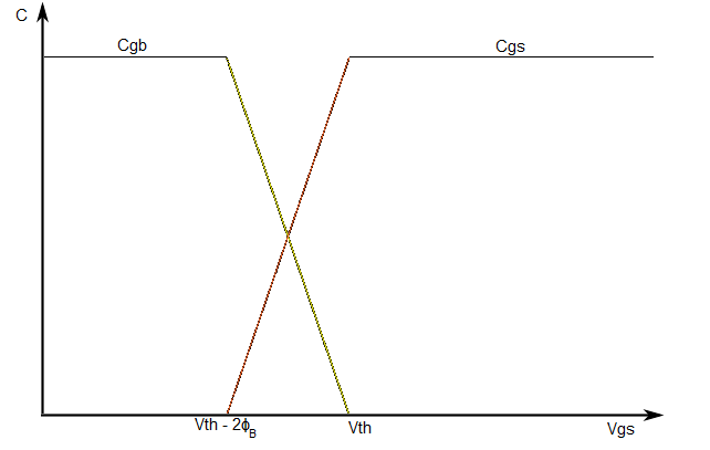
A simplified Meyer's capacitance model is used to describe the gate-source capacitance, CGS, the gate-bulk capacitance, CGB, and the gate-drain capacitance, CGD. These figures show how the gate-bulk and gate-source capacitances change instantaneously, while the

Gate-bulk and gate-source capacitance change instantaneously.

The two fixed capacitance options (Specify fixed input, reverse transfer and
output capacitance or Specify fixed gate-source, gate-drain and
drain-source capacitance) let you model gate capacitance as a fixed
gate-source capacitance CGS and either a fixed or
a nonlinear gate-drain capacitance CGD. If you
select the Gate-drain charge function is nonlinear option for the
Gate-drain charge-voltage linearity parameter, then the gate-drain
charge relationship is defined by the piecewise-linear function shown in the following
figure.

For instructions on how to map a time response to device capacitance values, see the N-Channel IGBT block reference page. However, this mapping is only approximate because the Miller voltage typically varies more from the threshold voltage than in the case for the IGBT.
Note
Because this block implementation includes a charge model, you must model the impedance of the circuit driving the gate to obtain representative turn-on and turn-off dynamics. Therefore, if you are simplifying the gate drive circuit by representing it as a controlled voltage source, you must include a suitable series resistor between the voltage source and the gate.
Representation by 2-D Lookup Table
For the lookup table representation of the detailed block modeling option, you provide tabulated values for source-drain currents as a function of source-gate voltage and source-gate voltage. The main advantage of using this option is simulation speed. It also lets you parameterize the device from either measured data or from data obtained from another simulation environment.
This figure shows the implementation of the 2-D lookup table option when you set
Isd-Vsd parameterization to Provide negative and
positive Vsd data:

This figure shows the implementation of the 2-D lookup table option when you set
Isd-Vsd parameterization to Provide positive Vsd data
only:

For the four terminal MOSFET, the surface potential and body factor values are calculated based on the nearest threshold voltage as shown in this picture:

Note
To ensure that the signs of the source-drain current and source-drain voltage are consistent:
If the source-drain voltage is equal to
0, the value of the Tabulated source-drain currents, Isd(Vsg,Vsd) parameter must be equal to0.The tabulated power, which is the product of the Tabulated source-drain currents, Isd(Vsg,Vsd) parameter and the source-drain voltage, must be greater than or equal to
0.The tabulated conductance, which is the gradient of the Tabulated source-drain currents, Isd(Vsg,Vsd) parameter with respect to the source-drain voltage Vsd, must be greater than or equal to
0.The first gradient of the Tabulated source-drain currents, Isd(Vsg,Vsd) parameter, with respect to source-gate voltage Vsg, must be equal to
0.
Representation by 3-D Lookup Table
For the temperature-dependent lookup table representation of the detailed block modeling option, you provide tabulated values for source-drain currents as a function of source-gate voltage, source-gate voltage, and temperature.
Note
To ensure that the signs of the source-drain current and source-drain voltage are consistent:
If the source-drain voltage is equal to
0, the value of the Tabulated source-drain currents, Isd(Vsg,Vsd,T) parameter must be equal to0.The tabulated power, which is the product of the Tabulated source-drain currents, Isd(Vsg,Vsd,T) parameter and the source-drain voltage, must be greater than or equal to
0.The tabulated conductance, which is the gradient of the Tabulated source-drain currents, Isd(Vsg,Vsd,T) parameter with respect to the source-drain voltage Vsd, must be greater than or equal to
0.The first gradient of the Tabulated source-drain currents, Isd(Vsg,Vsd,T) parameter, with respect to source-gate voltage Vsg, must be equal to
0.
Surface-Potential-Based Model
The surface-potential-based modeling option of the block provides a greater level of model fidelity than the simple square-law (threshold-voltage-based) model. The surface-potential-based block modeling option includes the following effects:
Fully nonlinear capacitance model (including the nonlinear Miller capacitance)
Charge conservation inside the model, so you can use the model for charge sensitive simulations
Velocity saturation and channel-length modulation
The intrinsic body diode
Reverse recovery in the body diode model
Temperature scaling of physical parameters
For the thermal modeling option, dynamic self-heating (that is, you can simulate the effect of self-heating on the electrical characteristics of the device)
This model is a minimal version of the world-standard PSP model (see https://briefs.techconnect.org/papers/introduction-to-psp-mosfet-model/), including only certain effects from the PSP model to strike a balance between model fidelity and complexity. For details of the physical background to the phenomena included in this model, see [2].
The surface-potential equation is derived similar to the way described on the N-Channel MOSFET block reference page, with all voltages, charges, and currents multiplied by -1.
The overall model consists of an intrinsic MOSFET defined by the surface-potential formulation, a body diode, series resistances, and fixed overlap capacitances, as shown in the schematic.


Modeling Body Diode
The block models the body diode either as an ideal, exponential diode or as a tabulated diode.
The block models the body diode either as an ideal, exponential diode or as a tabulated diode.
When you set Model body diode to
Exponential, the junction and diffusion capacitances
are:
where:
Idio is the current through the diode.
Is is the reverse saturation current.
VBD is the body-drain voltage.
n is the ideality factor.
ϕT is the thermal voltage.
Cj is the junction capacitance of the diode.
Cj0 is the zero-bias junction capacitance.
Vbi is the built-in voltage.
Cdiff is the diffusion capacitance of the diode.
τ is the transit time.
The capacitances are defined through an explicit calculation of charges, which are then differentiated to give the capacitive expressions above. The block computes the capacitive diode currents as time derivatives of the relevant charges, similar to the computation in the surface-potential-based MOSFET model.
To model a tabulated diode, set the Model body diode parameter to
Tabulated I-V curve. This figure shows the implementation of
the tabulated diode option:

When choosing this parameterization, you must provide the data for the forward bias only.
The block implements the diode using a smooth interpolation option. If the diode exceeds the provided tabulated data range, the block uses a linear extrapolation technique at the last voltage-current data point.
To specify the off conductance of the tabulated diode, set the Diode off conductance parameter. (since R2024a)
Note
The tabulated diode does not model the reverse breakdown.
Modeling Temperature Dependence
The default behavior is that dependence on temperature is not modeled, and the device is
simulated at the temperature for which you provide block parameters. To model the dependence
on temperature during simulation, select Model temperature
dependence for the Parameterization parameter in the
Temperature Dependence setting.
Threshold-Based Model
For threshold-based modeling option, you can include modeling the dependence of the transistor static behavior on temperature during simulation. Temperature dependence of the junction capacitances is not modeled, this being a much smaller effect.
When including temperature dependence, the transistor defining equations remain the same. The gain, K, and the threshold voltage, Vth, become a function of temperature according to the following equations:
Vths = Vth1 + α ( Ts – Tm1)
where:
Tm1 is the temperature at which the transistor parameters are specified, as defined by the Measurement temperature parameter value.
Ts is the simulation temperature.
KTm1 is the transistor gain at the measurement temperature.
KTs is the transistor gain at the simulation temperature. This is the transistor gain value used in the MOSFET equations when temperature dependence is modeled.
Vth1 is the threshold voltage at the measurement temperature.
Vths is the threshold voltage at the simulation temperature. This is the threshold voltage value used in the MOSFET equations when temperature dependence is modeled.
BEX is the mobility temperature exponent. A typical value of BEX is -1.5.
α is the gate threshold voltage temperature coefficient, dVth/dT.
For the four terminals parameterization, Vth is obtained using these equations:
| VBS Range | Vth Equation |
|---|---|
Where:
is the surface potential and .
Eg(0) is the extrapolated zero degree band-gap, which is equal to
1.16eVfor silicon.VBS is the bulk-source voltage.
For most MOSFETS, you can use the default value of -1.5 for
BEX. Some datasheets quote the value for α, but most
typically they provide the temperature dependence for drain-source on resistance,
RDS(on). Depending on the block parameterization
method, you have two ways of specifying α:
If you parameterize the block from a datasheet, you have to provide RDS(on) at a second measurement temperature. The block then calculates the value for α based on this data.
If you parameterize by specifying equation parameters, you have to provide the value for α directly.
If you have more data comprising drain current as a function of gate-source voltage for more than one temperature, then you can also use Simulink® Design Optimization™ software to help tune the values for α and BEX.
Surface-Potential-Based Model
The surface-potential-based model includes temperature effects on the capacitance characteristics, as well as modeling the dependence of the transistor static behavior on temperature during simulation.
The Measurement temperature parameter on the Main setting specifies temperature Tm1 at which the other device parameters have been extracted. The Temperature Dependence setting provides the simulation temperature, Ts, and the temperature-scaling coefficients for the other device parameters. For more information, see Temperature Dependence (Surface-Potential-Based Modeling Option).
Faults
To model a fault in the P-Channel MOSFET block, in the Faults section, click Add fault next to the fault that you want to model. For more information about fault modeling, see Fault Behavior Modeling and Fault Triggering.
The P-Channel MOSFET block models five types of fault:
Open circuit— Failure due to metallization burnoutDrain-source short— Failure due to avalanche breakdown on drain-source channelDrain-bulk short or source-bulk short— Failure due to avalanche breakdown on drain-bulk or source-bulk channelsGate oxide short— Failure of the gate oxide dielectric layerParameter shift— Failure due to aging
The block can trigger fault events at a specific time or when the current or voltage exceed the limit for longer than a specific time interval.
If, in the Faults settings, you set the Failure
mode parameter to Parameter shift, the MOSFET
fails due to the aging of its components. This equation defines the value of the shifted
parameters:
where tth is the time threshold when the fault is triggered and τ is the value of the Fault transition time constant, tau parameter.
If, in the Faults settings, you set the Failure
mode parameter to Gate oxide short, the gate oxide
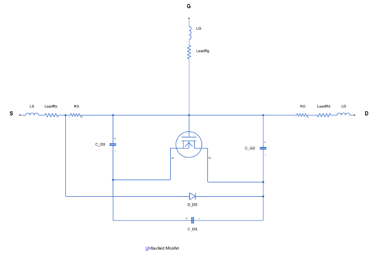
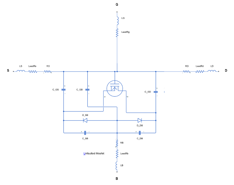
dielectric layer fails. These figures show the equivalent circuits for the three-terminal
MOSFET in the unfaulted and faulted state:


These figures show the equivalent circuits for the four-terminal MOSFET in the unfaulted and faulted state:


Thermal Port
The block has an optional thermal port, hidden by default. To expose the thermal port, set the Modeling option parameter to:
Threshold-based with thermal— Model based on threshold voltage and with exposed thermal portSurface-potential-based with thermal— Model based on surface potential and with exposed thermal port
This action displays the thermal port H on the block icon, and exposes the Thermal Port parameters.
Use the thermal port to simulate the effects of generated heat and device temperature. For more information on using thermal ports and on the Thermal Port parameters, see Simulating Thermal Effects in Semiconductors.
Variables
To set the priority and initial target values for the block variables before simulation, use the Initial Targets section in the block dialog box or Property Inspector. For more information, see Set Priority and Initial Target for Block Variables.
Use nominal values to specify the expected magnitude of a variable in a model. Using system scaling based on nominal values increases the simulation robustness. Nominal values can come from different sources. One of these sources is the Nominal Values section in the block dialog box or Property Inspector. For more information, see System Scaling by Nominal Values.
This table shows the relationship between the capacitances of the block and the initial targets:
| Defined Capacitance | Initial Targets |
|---|---|
| Gate-emitter capacitance, Cge | Set the initial target for the gate-emitter capacitance voltage only. Set the initial target of the collector-emitter capacitance voltage to 0 or set its priority to None. |
| Collector-emitter capacitance, Cce | Set the initial target for the collector-emitter capacitance voltage only. Set the initial target of the gate-emitter capacitance voltage to 0 or set its priority to None. |
| Gate-collector capacitance, Cgc | Set the initial targets for the gate-collector voltages by applying constraints on the gate-emitter and collector-emitter voltages. The initial condition of the gate-collector capacitance voltage is equal to the voltage between the gate-emitter and collector-emitter. |
| Gate-emitter capacitance, Cge, and gate-collector capacitance, Cgc | Set the initial targets for the gate-emitter and gate-collector voltages by applying constraints on the gate-emitter and collector-emitter voltages. The initial condition of the gate-collector capacitance voltage is equal to the voltage between the gate-emitter and the collector-emitter. |
| Gate-emitter capacitance, Cge, and collector-emitter capacitance, Cce | Set the initial target for the gate-emitter and the collector-emitter capacitance. |
| Gate-collector capacitance, Cgc, and collector-emitter capacitance, Cce | Set the initial targets for the gate-collector and collector-emitter voltages by applying constraints on the gate-emitter and collector-emitter voltages. The initial condition of the gate-collector capacitance voltage is equal to the voltage between the gate-emitter and the collector-emitter. |
| Gate-emitter capacitance, Cge, gate-collector capacitance, Cgc, and collector-emitter capacitance, Cce | Set the initial targets for the gate-emitter, gate collector and collector-emitter capacitances by applying constraints on the gate-emitter and collector-emitter voltages. The initial condition of the gate-collector capacitance voltage is equal to the voltage between the gate-emitter and the collector-emitter. |
Note
Inside your model, the number of initial targets with Priority equal to Low or High must match the number of differential variables. The differential variables come from the inductors and the capacitances in the model.
Plot Device Characteristics
You can plot the basic I-V characteristics of the P-Channel MOSFET block without building a complete model. Use the plots to explore the impact of your parameter choices on device characteristics. If you parameterize the block from a data sheet, you can compare your plots to the data sheet to check that you parameterized the block correctly. If you have a complete working model but do not know which manufactured part to use, you can compare your plots to data sheets to help you decide.
To plot the basic I-V characteristics, set the Modeling option
parameter to Threshold-based or
Surface-potential-based and, in the
Utilities section, click the
Plot button next to the Basic characteristics
parameter. (since R2026a) For more information about the Basic
characteristics parameter, see Plot Basic I-V Characteristics of Semiconductor Blocks.
You can also perform an in-depth study of the block characteristics and match the block
behavior to a set of target characteristics. To perform an in-depth study of the block
characteristics, set the Modeling option parameter to
Surface-potential-based and, in the
Utilities section, click the
Explore button next to the Characteristics
parameter. (since R2026a) For more information about the Characteristics
parameter, see MOSFET Characteristics Viewer.
Examples
Assumptions and Limitations
When modeling temperature dependence for threshold-based block modeling option, consider the following:
The block does not account for temperature-dependent effects on the capacitances.
When you specify RDS(on) at a second measurement temperature, it must be quoted for the same working point (that is, the same drain current and gate-source voltage) as for the other RDS(on) value. Inconsistent values for RDS(on) at the higher temperature will result in unphysical values for α and unrepresentative simulation results. Typically RDS(on) increases by a factor of about 1.5 for a hundred degree increase in temperature.
You may need to tune the values of BEX and threshold voltage, Vth, to replicate the IDS–VGS relationship (if available) for a given device. Increasing Vth moves the IDS–VGS plots to the right. The value of BEX affects whether the IDS–VGS curves for different temperatures cross each other, or not, for the ranges of VDS and VGS considered. Therefore, an inappropriate value can result in the different temperature curves appearing to be reordered. Quoting RDS(on) values for higher currents, preferably close to the current at which it will operate in your circuit, will reduce sensitivity to the precise value of BEX.
Ports
Conserving
Parameters
References
[1] Shichman, H. and D. A. Hodges. “Modeling and simulation of insulated-gate field-effect transistor switching circuits.” IEEE J. Solid State Circuits. SC-3, 1968.
[2] Van Langevelde, R., A. J. Scholten, and D. B. M. Klaassen. "Physical Background of MOS Model 11. Level 1101." Nat.Lab. Unclassified Report 2003/00239. April 2003.
[3] Oh, S-Y., D. E. Ward, and R. W. Dutton. “Transient analysis of MOS transistors.” IEEE J. Solid State Circuits. SC-15, pp. 636-643, 1980.


