Thyristor
Thyristor using NPN and PNP transistors
Libraries:
Simscape /
Electrical /
Semiconductors & Converters
Description
The Thyristor block provides two ways of modeling a thyristor:
As an equivalent circuit based on NPN and PNP bipolar transistors
By a lookup table approximation to the on-state I-V (current-voltage) curve
Representation by Equivalent Circuit
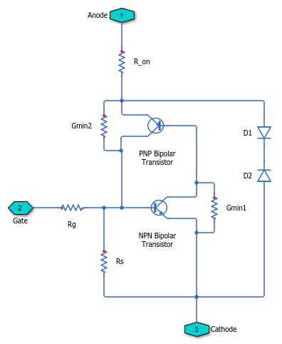
The equivalent circuit contains a pair of NPN and PNP bipolar transistors, as shown in the following illustration.

The P-N-P-N structure of a thyristor is matched by the P-N-P and N-P-N structures of the bipolar transistors, the base of each device being connected to the collector of the other device. To ensure that this circuit behaves like a thyristor, it is necessary to pick suitable parameter values of the NPN and PNP devices, plus external resistors. For example, for the circuit to latch into the on-state, once triggered by a suitable gate current, the total gain of the two transistors must be greater than one. This model structure replicates the behavior of a thyristor in typical application circuits, while at the same time presenting a minimum number of equations to the solver, to improve simulation speed.
Note
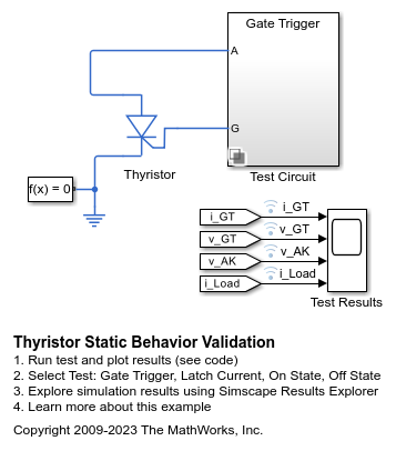
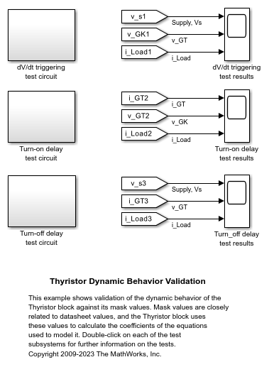
It is extremely important that you parameterize the thyristor component correctly before using it in your model. To help you do this, there are two test harnesses in the Simscape™ Electrical™ examples, Thyristor Static Behavior Validation and Thyristor Dynamic Behavior Validation. Follow the help text for these two examples, plus a datasheet for your device, to re-parameterize the thyristor component so that it replicates the required behavior. You can then copy the parameterized component into your model. Take care to model the gate drive circuitry correctly, including circuit series resistance. Connecting a controlled voltage source directly to the thyristor gate gives nonphysical results because it clamps the gate to the cathode voltage when the gate demand is zero.
The model captures the following thyristor behaviors:
Off-state currents, IDRM and IRRM. These are typically quoted for the maximum off-state voltages VDRM and VRRM. It is assumed, as is the case for most thyristors, that IDRM = IRRM and VDRM = VRRM.
The gate trigger voltage is equal to the Corresponding gate voltage, V_GT parameter value when the gate current is equal to the Gate trigger current, I_GT parameter value.
The thyristor latches on when the gate current is equal to the Gate trigger current, I_GT. The thyristor does not latch on until the gate current reaches this value. To ensure this is the case, you must set the Internal shunt resistor, Rs parameter correctly. If the resistance is too high, then the gate triggers before the gate current reaches iGT. If the resistance is too small, then the gate does not trigger.
You can determine the value of the internal shunt resistor Rs by running the simulation. To see how this can be done, refer to the Thyristor Static Behavior Validation example. Alternatively, if you are using the thyristor in a circuit where there is an external resistor RGK connected from gate to cathode, then the effect of Rs is usually very small, and it can be set to
inf.With the thyristor in the on-state, if the gate current is removed, the thyristor stays in the on-state, provided that the load current is higher than the holding current. You do not specify the holding current directly because its value is primarily determined by other block parameters.
However, the holding current can be influenced by the Product of NPN and PNP forward current gains parameter on the Advanced tab. Reducing the gain increases the holding current.
The on-state voltage is equal to the On-state voltage, V_T parameter value when the load current is equal to the On-state current, I_T parameter value. This is ensured by the R_on resistance value, which takes into account the voltage drop seen across the PNP and NPN devices.
Triggering by rate of rise of off-state voltage. A rapid change in anode-cathode voltage induces a current in the base-collector capacitance terms. If this current is large enough, it triggers the thyristor into the on-state. The thyristor initialization routine calculates a suitable value for the base-collector capacitance, so that when the rate of change of voltage is equal to the Critical rate of rise of off-state voltage, dV/dt parameter value, the thyristor triggers on. This calculation is based on the approximation that the required current is vGT / RGK where RGK is the gate-cathode resistance value used when quoting the critical dV/dt value.
A nonzero gate-controlled turn-on time, primarily influenced by the NPN device forward transit time, TF. You either specify this parameter directly, or calculate an approximate value for TF from the turn-on time.
A nonzero commuted turn-off time, primarily influenced by the PNP device forward transit time, TF. You can either specify this parameter directly, or set it to be equal to the forward transit time for the NPN transistor.
Resistors Gmin1 and Gmin2 improve numerical robustness at large forward and reverse voltages. Their values influence the off-state currents by no more than 1% at the maximum off-state forward and reverse voltages.
Note
Because this block implementation includes a charge model, you must model the impedance of the circuit driving the gate to obtain representative turn-on and turn-off dynamics. Therefore, if you are simplifying the gate drive circuit by representing it as a controlled voltage source, you must include a suitable series resistor between the voltage source and the gate.
Representation by Lookup Table
If using the lookup table representation, you provide tabulated values for anode-cathode current as a function of anode-cathode voltage when in the on state. The main advantages of using this option are simulation speed and ease of parameterization. To further simplify the underlying model, this representation does not model:
Device triggering due to rate of rise of off-state voltage
Commuted turn-off time
The turn-on delay is represented by an input gate-cathode capacitor, the value of which is calculated so that the delay between gate voltage rising and the device starting to turn on is equal to the value specified by the Turn-on delay time parameter. The turn-on rise time for the load current is implemented by ramping nonlinearly between zero and the current determined by on-state current-voltage profile over a time period specified by the value of the Turn-on rise time parameter. Note that the resulting turn-on current profile is an approximation to an actual device.
Thermal Port
You can expose the thermal port to model the effects of generated heat and device temperature. To expose the thermal port, set the Modeling option parameter to either:
No thermal port— The block does not contain a thermal port and does not simulate heat generation in the device.Show thermal port— The block contains a thermal port that allows you to model the heat that conduction losses generate. For numerical efficiency, the thermal state does not affect the electrical behavior of the block.
For more information on using thermal ports and on the Thermal Port parameters, see Simulating Thermal Effects in Semiconductors.
Variables
To set the priority and initial target values for the block variables before simulation, use the Initial Targets section in the block dialog box or Property Inspector. For more information, see Set Priority and Initial Target for Block Variables.
Use nominal values to specify the expected magnitude of a variable in a model. Using system scaling based on nominal values increases the simulation robustness. Nominal values can come from different sources. One of these sources is the Nominal Values section in the block dialog box or Property Inspector. For more information, see System Scaling by Nominal Values.
Examples
Assumptions and Limitations
This block does not model temperature-dependent effects. This block is simulated at the temperature specified by the Measurement temperature parameter value. All parameters must be quoted for this temperature.
If you use the equivalent circuit representation:
In sensitive gate circuits (that is, where there is no external gate-cathode resistor RGK), you must set the value of the Internal shunt resistor, Rs parameter to ensure correct triggering. If the internal shunt resistance is too high, then the thyristor triggers for currents less than iGT. If the internal shunt resistance is too low, the thyristor does not trigger for an input current of iGT. For details on using simulation to determine the acceptable internal shunt resistance value, see the Thyristor Static Behavior Validation example.
Triggering by exceeding the breakover voltage is not modeled.
Numerically the thyristor can be demanding to simulate, given the very small gate currents in comparison to the load current, and also the very steep current gradients during switching. However, for most typical thyristor-based circuits, you can use the default simulation parameters. In some cases you may need to tighten the Absolute Tolerance and Relative Tolerance parameters on the Solver tab of the Configuration Parameters dialog box, to ensure convergence. In such cases, changing the default value of Absolute Tolerance from
autoto1e-4or1e-5is usually sufficient, because it prevents adaptive changing of this parameter during simulation.The leakage currents are approximated by the diodes D1 and D2, as shown in the equivalent circuit. This approach assumes that the leakage via the two transistors is small in comparison. This assumption is not valid for values of vGT that are significantly smaller than the typical forward voltage drop of 0.6 V.
If you use the lookup table representation:
Triggering by exceeding the breakover voltage or by rate of change of off-state voltage is not modeled.
Commutated turn-off time is not modeled. Check that your circuit does not violate the stated commutated turn-off time for the thyristor.
When you specify a turn-on rise time, the resulting current-time profile is an approximation.
Ports
Conserving
Parameters
References
[1] G. Massobrio and P. Antognetti. Semiconductor Device Modeling with SPICE. 2nd Edition, McGraw-Hill, 1993.


