Get Started with RAM and ROM in Simulink
R2026bThis example shows how to configure RAM blocks in Simulink® to generate synthesizable HDL code by using HDL Coder™. The generated code can be mapped by synthesis tools to dedicated RAM resources available in FPGA devices. This example also shows how to model ROM behavior in Simulink.
RAM Blocks in the HDL Example Library
HDL Coder includes several RAM blocks in the HDL RAMs library. Use the hdllib command to display blocks that are compatible with HDL Coder in the Library Browser. In the Library Browser, navigate to HDL Coder > HDL RAMs to access these blocks.
The library includes:
These RAM blocks are masked subsystems that support behavioral simulation in Simulink. During HDL code generation, HDL Coder replaces these subsystems with predefined HDL templates that describe the RAM structures. Most synthesis tools recognize these templates and map them to dedicated FPGA RAM resources.
Use Generic RAM Coding Style for RAM Blocks
By default, HDL Coder implements RAM templates that use a dedicated clock enable signal for the RAM structures. Alternatively, you can use the generic RAM coding style templates, which removes the clock enable port and implements clock enable behavior by using additional wrapper logic around the RAM. You can control this behavior by using the RAM Architecture model configuration parameter.
Use the generic RAM style when the synthesis tool does not support RAM blocks with a clock enable signal or cannot map the clock enabled RAMs to dedicated FPGA memory resources.
The hdlcoderfirram model shows how to use the generic RAM coding style in a design.
open_system("hdlcoderfirram");
open_system("hdlcoderfirram/FIR_RAM");
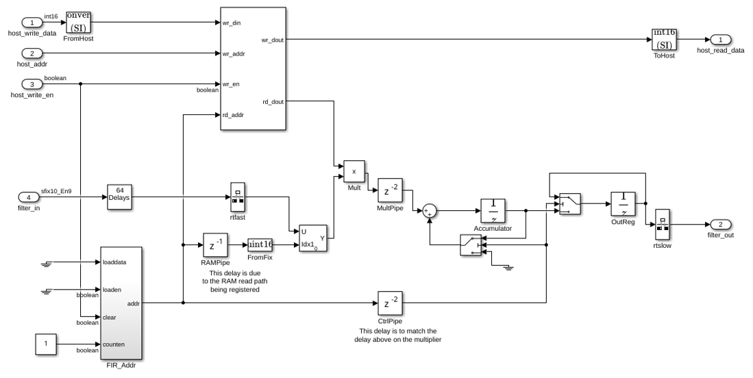
Select RAM Coding Style
You can select the RAM coding style from the Configuration Parameters dialog box:
1. In the Simulink Toolstrip, on the Apps tab, select HDL Coder.
2. On the HDL Code tab, click Settings.
3. In HDL Code Generation > Global Settings > Coding style, set the RAM Architecture parameter to your desired RAM coding style.
You can use the RAM Architecture parameter to control how HDL Coder generates the clock enable port for RAM in a subsystem.
When you set RAM Architecture to
RAM with clock enable, HDL Coder generates code with a clock enable port for the RAM.When you set RAM Architecture to
Generic RAM without clock enable, HDL Coder generates RAM without a clock enable port and inserts a wrapper that implements the required clock enable logic.
To suppress the generation of clock enable logic in the design, use the Minimize clock enables model configuration parameter.
The RAM Architecture and the Minimize clock enables parameters determine how HDL Coder generates clock enable port on RAM inside a subsystem and at the top-level DUT.
        RAM Architecture Setting        Minimize Clcok Enables Setting    Clock Enable at Top-level DUT    Clock Enable on RAM
    ________________________________    ______________________________    _____________________________    ___________________

    RAM with clock enable                    Selected                                  No                          No
    RAM with clock enable                    Cleared                                   No                          Yes
    Generic RAM without clock enable         Selected or Cleared                       Yes                         No
Build ROM Using Simulink Blocks
HDL Coder does not include a dedicated ROM block, but you can build one by using a Lookup Table block together with a Unit Delay block.
open_system("hdlcoderrom");
open_system("hdlcoderrom/ROM");
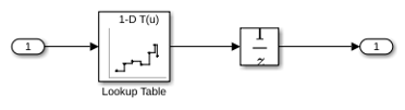
When building a ROM model in Simulink, follow these guidelines:
For an n-bit address, specify all
 entries of the lookup table data. If any entries are missing, the synthesis tool may not infer RAM, and the generated HDL code may not match the simulation behavior.
Place the Lookup Table and Unit Delay blocks at the same hierarchy level in the model.
Support for RAM reset logic varies across FPGA devices and synthesis tools. To achieve the best synthesis results, suppress the generation of reset logic for the Unit Delay block by setting its Reset type property to
nonein the HDL Block Properties dialog box. Also, set the Ignore output data checking (number of samples) property to1to avoid the initial simulation mismatch caused by the suppressed reset logic.
If you follow these guidelines, most synthesis tools implement the ROM using dedicated RAM resources in an FPGA.
Minimum RAM Size Requirements
When the RAM or ROM structure size in your design is small, synthesis tools may map the generated code to registers instead of block RAM to improve performance. Check the synthesis tool documentation for the minimum RAM size required for block RAM inference and for any available options that allow you to override the default mapping behavior.

